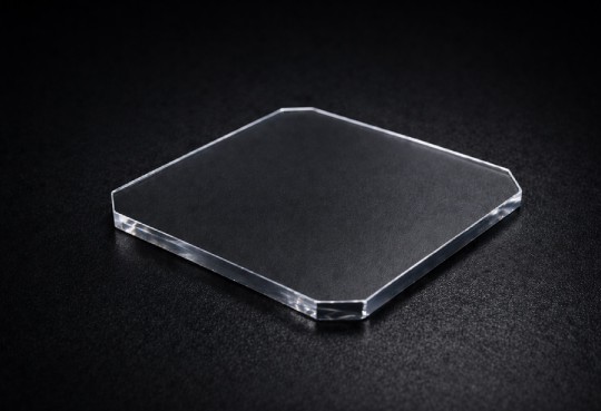
Single Crystal CVD Diamond
Maximum thermal conductivity and crystal quality — for the most demanding RF and semiconductor performance applications.
Advanced GaN semiconductor wafers, GaN-on-Diamond and CVD diamond substrates — built for high-power electronics, RF systems, quantum technologies, and advanced computing, where thermal performance decides everything.
Gallium nitride epitaxial structures, integrated directly with diamond substrates. The result: dramatically better thermal conductivity, higher power density, and improved device reliability across advanced semiconductor applications.
It is the substrate platform for devices that run hotter, faster, and denser than silicon was ever designed to handle.
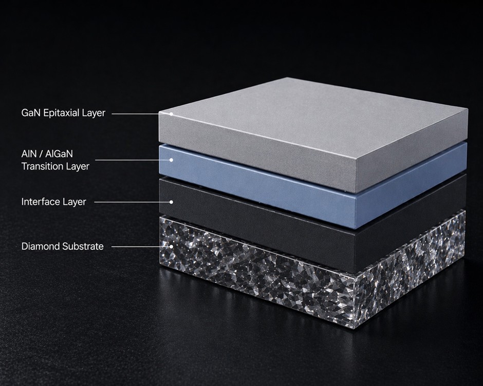
Gallium Nitride — GaN — is an advanced wide-bandgap semiconductor material used in high-performance electronic, power, radio frequency, photonic and sensing applications.
As industries move toward electrification, AI infrastructure, high-speed communications, compact power systems and secure defence technologies, traditional silicon platforms are being pushed past their limits. Devices now demand:
Our GaN semiconductor wafers give manufacturers, research organisations and technology developers an advanced wafer platform for next-generation devices.
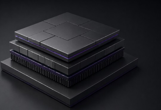
Diamond substrates significantly outperform every traditional semiconductor material at moving heat away from the device.
Thermal conductivity, W/m·K — typical room-temperature values.
Maximum thermal conductivity and crystal quality — for the most demanding RF and semiconductor performance applications.
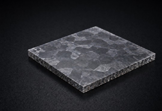
Engineered for thermal management at scale — optimised for high-volume semiconductor manufacturing environments.
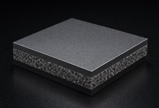
Advanced composites for enhanced thermal dissipation across high-power semiconductor systems.
QCT defines the substrate architecture, controls programme specifications, and aligns global manufacturing execution — so performance, scalability, and continuity hold from prototype to volume supply.
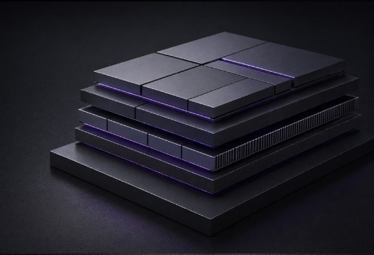
Engage with QCT to align advanced semiconductor materials and substrate platforms with your application requirements.
Initiate programme discussion →